BJT Transistor Biasing Calculator
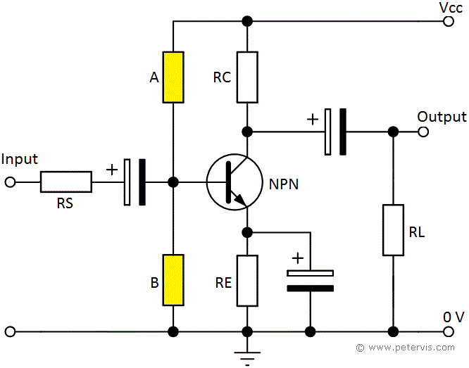
This calculator will compute the values of the biasing resistors required to provide the maximum output voltage swing in a NPN bipolar junction transistor (BJT) amplifier circuit. The algorithm makes use of AC and DC load line theory and formulas and is one of the most accurate you will find online. The circuit above is that of a typical common emitter amplifier with resistors at the emitter junction, and collector junction. Engineers usually need to calculate the values of resistors R1 and R2 so that the transistor provides maximum undistorted output. The algorithms I use here will also find the operating point (Q), which is useful if you are a student making calculations by hand.
Although there are many different techniques to biasing a transistor, I think that this is the most elegant one because it is practical and useful when designing circuits for amplification purposes. If you are designing amplifier stages using small signal transistors, then this ought to be the first place to start with the design because it will save you from some of the mathematics required.
Circuit Parameters
Capacitors
In this circuit, RL is the input impedance of the following stage decoupled by a capacitor. Capacitors present themselves as open circuit to DC voltages; however, they present themselves as short to AC voltages. The capacitor across RE bypasses the resistor thereby increasing the gain of the amplifier. The value of this capacitor is chosen such that at the operating frequency, its impedance is much lower than the value of RE.
These capacitors are usually electrolytic and low in value, typically 4.7 µF, however there is a calculator for this that I shall be adding in the future if anyone is interested.