Raspberry Pi Pinout
The General Purpose Input / Output (GPIO) pinout is almost the same for Rev 1 and Rev 2 versions of the Raspberry Pi due to them having the same BCM2835 processor. This article documents the pinouts for the first version, and the second version called revision 2. It also includes the serial pins and the I2C pins, including printable PDF diagrams for classroom use.
GPIO
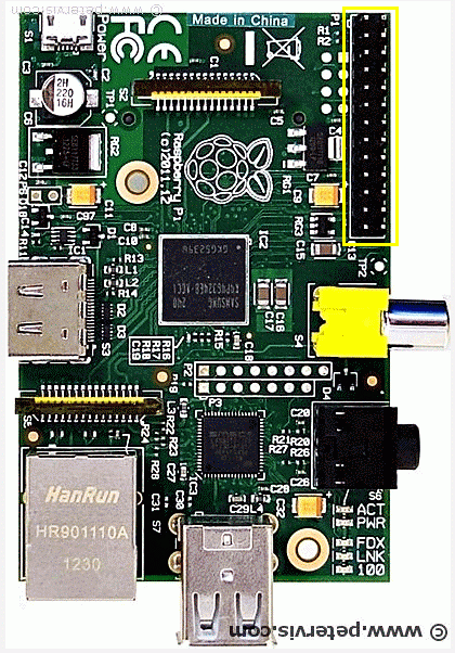
The diagram above shows the P1 header consisting of GPIO pins. Pin 1 is marked on the board and indicated by the diagram. Please note that the GPIO pins are very sensitive to voltages and that this is a 3.3 V logic system. The following section of this article documents their electrical characteristics and interfacing requirements.
GPIO Pinout Diagram
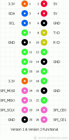
Here is a diagram showing the functional arrangement of the pins. After analysing the circuit diagrams, I found that the functional arrangement with respect to the serial, I2C, and the power pins is the same for both the first version of the Raspberry Pi and for the second version called revision 2. The main difference between the two versions is in the GPIO designations of the pins.
The colouring scheme of the functional arrangement is the same as that shown on the Broadcom datasheet, which is the best one to use.
Version 1 GPIO Pinout
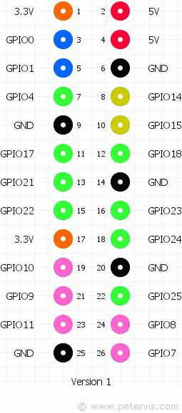
This is the diagram of the first version (Version 1) of the Raspberry Pi showing the functional arrangement by colour, and the GPIO designations.
Revision 2 GPIO Pinout
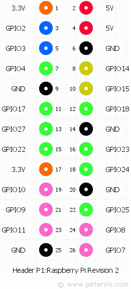
This is the second version (revision 2) of the Raspberry Pi board, also known as Rev2, or V2. As you can see from the colours that the functional arrangement is the same as that of Version 1, however the GPIO designations are slightly different. In revision 2 there is also a second header socket called P5, which contains additional GPIO pins.
P5 Socket
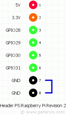
The second version of the Raspberry Pi (revision 2) has an additional header marked P5. This contains more GPIO lines as well as the power and ground pins. I managed to figure out how it maps as shown above.
Most people tend to overlook this header but it is very useful if you need additional GPIO pins for a project.
Serial SPI

This diagram shows the serial communication pins, which is the same for both versions of the Raspberry Pi. SPI_MOSI (pin 19), SPI_MISO (pin 21), SPI_SCLK (pin 23), for the communication, and SPI_CE0 (pin 24), SPI_CE1 (pin 26) are the chip enable pins. For more information, please see my excellent Raspberry Pi SPI article.
I2C Pins on GPIO
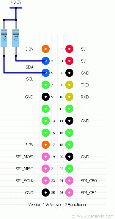
The I2C pinout is very simple as the bus uses two pins SDA (pin 3), and SCL (pin 5). Resistors R1 and R2 pull these pins high to the 3.3 V rail. This arrangement is the same on both versions of the board.
Power Pins
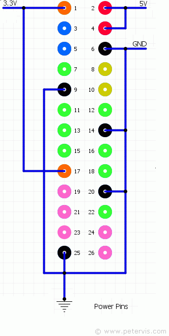
The locations of the power and ground pins are as shown in the diagram above. The officially recommended pins are pin 1 (+3.3 V), pin 2 (+5 V), and pin 6 (Ground). The rest of the pins are not usually used.
GPIO PDF
All graphics are copyright protected. All rights reserved. However, paper based school use is allowed.
| Raspberry Pi GPIO | raspberry_pi_pinout.pdf |
| Rev 1 | raspberry_pi_pinout_version_1.pdf |
| Rev 2 | raspberry_pi_pinout_rev2.pdf |
This Article Continues...
Raspberry Pi GPIO CableRaspberry Pi Blink LED
Raspberry Pi Board B GPIO Header