ATmega32: Building an ISP Serial cable
This in-system programming (ISP) cable is a programmer, which enables the 32 KB program memory of the ATMega32 to be reprogrammed in-system through the serial peripheral interface (SPI). This interface facilitates the connection and high-speed synchronous data transfer between the ATMega32 and a computer for flashing the memory. The circuit uses the MISO, MOSI, and SCK pins to provide a synchronous data transfer, which the reset pin initiates. This is an extremely simple circuit, which requires a prototyping board for mounting the components. You could build it within the DB9 casing or within the target system with jumpers to isolate the SPI pin connection.
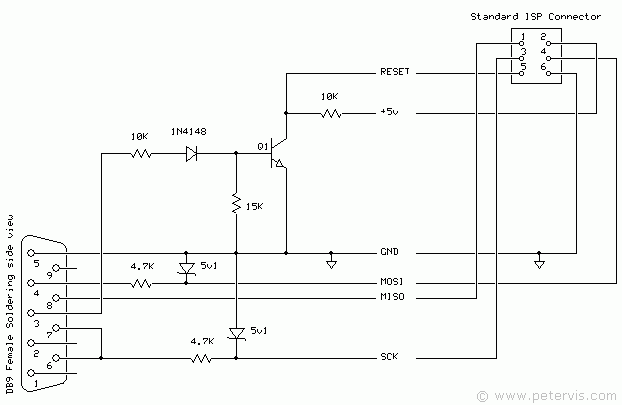
Circuit Diagram
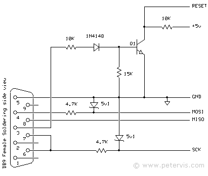
Originally, I was using a borrowed STK500; however, with the emergence of PonyProg software, building your own becomes a more cost effective option. I like the idea of building my own ISP cable because you achieve a deeper understanding of how the microcontroller works. This circuit is a simplified version compatible with SI Prog as used by the PonyProg flashing software.
RESET
The RESET pin is internally pulled up, and in most applications, this is sufficient. If your application is to work in a noisy RF environment, you may need to connect an external 10 kΩ resistor to provide an additional pull-up. This will prevent the system from resetting spuriously.
According to the "Atmel Hardware Design Considerations Paper", RESET is for the following purposes.
- To release all I/O by tri-stating all the pins
- To enter into programming mode
The ATmega32 RESET pin is active LOW, which means that for a reset to occur you must bring the pin to ground level.
Transistor
In this application, we are using the transistor as a switch. The signal from pin 3 (DB9) is used to switch the transistor Q1. When Q1 is conducting, the reset pulls low. Q1 can be almost any NPN general-purpose switching transistor. The most common ones are the BC546, BC547, BC548, BC549, and BD550, which could also be used, as well as many others.
Diodes
Since voltage levels on pin 3 can range from +15 V to -15 V, the diode 1N4148 blocks any negative voltage swings. In this application, almost any rectifier diode will work as long as it can withstand the voltage. However, if you have some low forward-voltage Schottky diodes, then those are better.
The Zener diode with a series resistor of 4.7 kΩ resistor forms a positive voltage regulator to clamp the voltage within TTL range of 5.1 V for SCK and MOSI signals.
Circuit Build
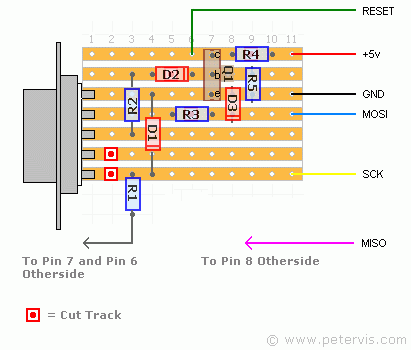
The prototyping board sandwiches between the two rows of pins and the top five pins align perfectly with the strips, therefore I decided to install the socket this way. In addition, I had to cut the strips to isolate pin 1 and pin 2 shown by the red squares. Remember, you also need to cut the strips under R4, R3, and D2.
The MOSI line connects directly to pin 9 of the DB9, which is on the reverse side, and not shown. A small jumper wire connects one of the resistor (R1) terminals to pin 7 and pin 6 which is also on the other side of the board.
| Component List | Value |
| R1 | 4.7 kΩ |
| R2 | 10 kΩ |
| R3 | 4.7 kΩ |
| R4 | 10 kΩ |
| R5 | 15 kΩ |
| D1 | 5.1 V |
| D2 (ZENER) | IN4148 |
| D3 (ZENER) | 5.1 V |
| Q1 | BC547 |
Power Supply
The +5 V comes from the Atmega32 voltage rail since that is where the most stabilised power will be. I considered taking power directly from the serial port (DB9) as I did in my Nokia M Bus Serial Cable circuit; however, it is unnecessary, since +5 V is readily available from the main board
DB9 Female Socket (Serial Socket)
In the schematic above, you are looking at the socket from the back where you solder the wires onto the pins. When you look at the socket from the back (soldering side), pin 1 is on the top left side. Wire the socket exactly as you would see it on the schematic above.
ISP Six Pin Header Standard
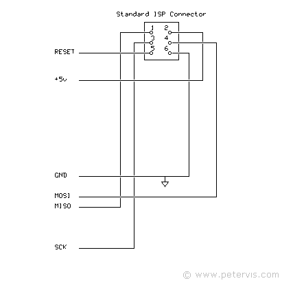
I am using the 6-pin layout standard as documented by Atmel in their "Hardware Design Considerations" paper, and the STK500 programmer uses this scheme as well. As I am using a recycled header socket with a ribbon cable already attached to it, I simply have to connect the other end of the ribbon cable to my circuit board to match the layout as shown below.
Transistor Pinout
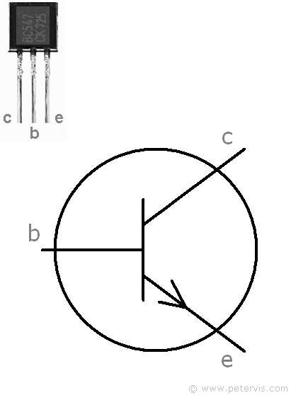
Here is a handy diagram to save time figuring out the BC547 A/B/C pinout. The BC546, BC547, BC548, BC549, and BD550 pinout is the same on the TO-92 package.
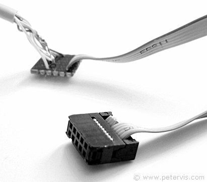
Ribbon Cable Wiring
I always use recycled components whenever I can, and this header socket is recycled from a computer motherboard. It is a female socket with ten pins; however, I shall be using only six of those pins.
I am using solid core copper wire I recycled from a CAT5 network cabling. This type of cable exhibits a low attenuation and is very durable. It has four pairs, and I am using a pair for +5 V and a pair for ground, leaving the rest for signals.
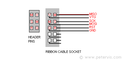
The diagram on the RHS shows the ribbon cable connections. The view is from the side with holes. As a result, it is a mirror image to the header pin configuration on the main board. The ribbon cable has a red wire on the far edge, which indicates the MISO line. Many online electronics shops sell DB9 cases, which are worth getting; however, I like my ISP cable just as it is.